In vision inspection, laser and optical sensing equipment, PCB boards, CMOS sensors, photodetectors and signal chips are typical ESD-sensitive components. Hidden damage caused by electrostatic discharge is tricky: instruments pass factory tests but develop intermittent faults or signal drift after transit. Without obvious burn marks, these latent defects often emerge after delivery to customers, bringing high after-sales cost and reputational risk. Therefore ESD protection is an essential part of packaging design for precision instruments.
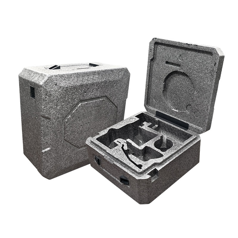
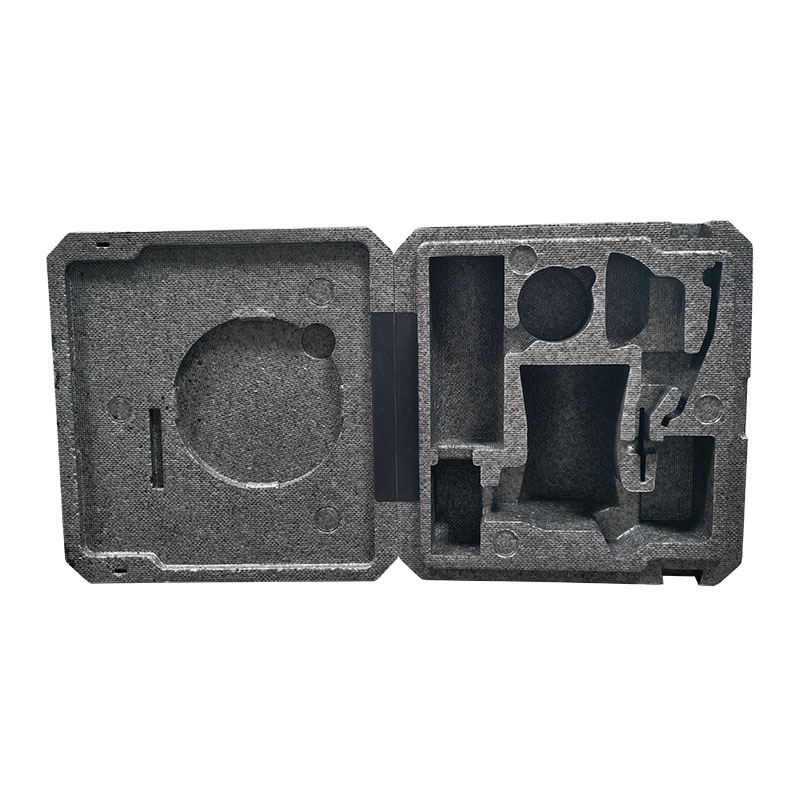
Standard EPP is inherently insulating and prone to static charge accumulation. Friction between parts and packaging during handling, stacking and transportation can build static electricity, and sudden discharge may permanently damage semiconductor devices. Modified anti-static EPP is produced by mixing approved anti-static additives into EPP beads before steam molding. The finished material maintains surface resistance within the ESD safe range of 10⁶–10⁹ Ω, draining static safely without creating short-circuit risks.
It is critical to distinguish bulk-modified EPP from spray-coated anti-static foam. Coating is only attached to the surface. After repeated rubbing and abrasion, the coating wears off quickly, losing ESD function and shedding dust particles that contaminate optical lenses.
For bulk-modified EPP, anti-static additives are distributed evenly inside the foam matrix. Even after long cycles and minor surface scuffing, ESD performance remains consistent. Combined with mold texturing, it achieves both anti-static property and dust-free requirement without extra painting, which fits optical assemblies with both lenses and electronic boards.
The molding process supports zoned multi-functional design. One single box can have anti-static EPP cavities for PCBs and sensors, paired with standard dust-free EPP zones for optical lenses. All structures are molded in one shot without adhesive bonding, keeping tight tolerances and separating protection levels for different components.
Anti-static EPP inherits the weather resistance of standard EPP: closed-cell structure with low water absorption and wide temperature tolerance. Its ESD performance will not fluctuate sharply under temperature cycling and high humidity inside sea freight containers. Compared with anti-static EVA or EPE, it has better creep resistance and longer service life for repeated circulation, aligning with ESG circular packaging targets.
Even with anti-static EPP, it cannot form a full ESD protection system alone. It serves as a static-dissipative carrier. Complete ESD control requires matching ESD shielding bags, grounded workstations and operator anti-static gear. For ultra-sensitive chips, the common practice is to seal components inside shielding bags before placing them into anti-static EPP cavities.
As for scenario selection: spray-coated foam is cheaper for one-off shipments with low ESD risk. Bulk-modified anti-static EPP brings stable long-term value for high-value sensors, cleanroom workflows, recurring repair circulation and overseas exports. Reliable suppliers carry out regular surface resistance sampling besides drop and vibration tests, verifying ESD stability after aging.
FAQ
Q1: Does anti-static EPP lose its function over time?
A: Bulk-modified EPP has anti-static additives embedded in the material, so degradation is slow under normal use. Spray-coated foam fails easily once the surface coating wears away. Periodic resistance testing is recommended.
Q2: Can anti-static EPP be dust-free for optical assemblies?
A: Yes. Mold-etched textured anti-static EPP without post-spraying avoids coating shedding and meets cleanroom standards.
Q3: Can one package combine anti-static zones and normal EPP zones?
A: Yes. Separate feeding during molding creates differentiated zones: anti-static for electronics and clean standard EPP for lenses.
Q4: Can anti-static EPP replace ESD shielding bags?
A: No. Anti-static EPP dissipates surface static charge but provides no electromagnetic shielding. High-sensitivity chips still require inner shielding bags.
Hidden ESD damage is a persistent quality risk for precision electronics. Anti-static EPP integrates cushioning, dust control and static dissipation in one reusable package, protecting high-value optical and electronic instruments. Fumei New Materials customizes bulk-modified anti-static EPP packaging with zoning and textured dust-free options, supported by surface resistance inspection, drop, vibration and damp-heat reliability tests.